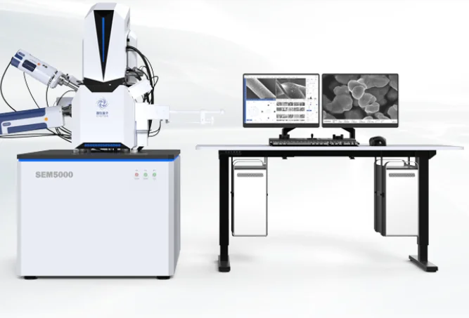
In modern research labs, imaging at the micro‑ and nano‑scale is essential across many disciplines. Among the tools enabling this, the Scanning Electron Microscope (SEM) stands as one of the most versatile. While field‑emission guns (FEGs) often get attention for highest resolution, tungsten filament SEMs remain highly relevant — especially when optimised for ultra‑high resolution. In this post, we explore what ultra‑high resolution tungsten filament SEMs are, how they work, their strengths & limitations, and the many ways labs are using them.
What is a Tungsten Filament SEM, and What Does “Ultra‑High Resolution” Mean
A tungsten filament SEM uses a heated tungsten wire as its electron source (often a thermionic emission source). When the filament is heated, electrons are emitted; these are accelerated, collimated, focused, and scanned over the sample. Detectors pick up various resulting signals (secondary electrons, backscattered electrons, etc.) to build up high‑magnification images of surfaces and near‑surface features.
“Ultra‑high resolution” in this context refers to achieving the finest possible detail (smallest resolvable features), often down towards a few nanometers. While classic tungsten filament SEMs might only reach ~20‑nm resolution under certain operation parameters, advances in electron optics, improved detection (e.g. better secondary electron detectors), better vacuum systems, clever lens design, and low‑voltage operation enable modern tungsten SEMs to approach or even surpass earlier depth/contrast limits.
Key Features & Technical Aspects
Here are important technical parameters and configurations that help define an ultra‑high resolution tungsten SEM and what labs should consider:
- Electron source: Tungsten filament (hairpin, coil, etc.), pre‑aligned to reduce aberrations. While not as bright and narrow as field emission sources, they are simpler and more robust.
- Acceleration voltage: The voltage that accelerates electrons determines beam energy and penetration. Lower voltages often help surface sensitivity and reduce sample damage, but may reduce resolution unless optical design compensates. Many tungsten SEMs are now offering low‑voltage capability.
- Vacuum system: High and stable vacuum is critical for minimizing electron scattering in the column, thus preserving beam coherence and sharpness. Vacuum levels in high‑resolution tungsten SEMs are typically very good (e.g., better than ~10⁻⁴ to 10⁻⁵ Pa).
- Detectors: Secondary electron detectors (for surface topology), backscattered electron detectors (for composition contrast), energy dispersive X‑ray spectroscopy (EDS) for elemental mapping, sometimes combined with other detectors like EBSD or cathodoluminescence for more advanced characterization.
- Magnification & Depth of Field: These microscopes can provide very high magnifications (hundreds of thousands ×) and excellent depth of field (important for 3D texture of surface features).
- Sample stage & environmental modes: Good stages with multiple axes, tilt, rotation; sometimes low vacuum/variable pressure modes or “environmental SEM” to handle less conductive or “wet” samples without heavy coating.
Advantages & Limitations
Advantages
- Cost‑Effectiveness
Tungsten filament SEMs are generally less expensive to purchase, maintain, and operate than field emission or LaB₆ sources. For many labs, especially in universities or developing regions, this makes them a more accessible route to high‑resolution imaging. - Robustness & Easier Maintenance
Filament sources are simpler and more resilient against failures. While they may require replacement of the filament and alignment, they are more forgiving in “field” or multi‑user lab settings. - Broad Sample Compatibility
Because they can be operated under various voltages, sometimes in low vacuum, and with multiple detector options, tungsten SEMs can handle metals, polymers, geological samples, ceramics, and even some biological or environmental samples (often with coatings or preparation). - Good Surface Topography & Depth of Field
For observing detailed surface morphology, fracture surfaces, inclusions, grain structure, coatings, and interfaces, tungsten SEMs excel. - Modularity & Accessory Integration
Many modern tungsten SEMs come with upgrade paths: better detectors (BSE, EDS), EBSD, etc. This allows labs to start with a basic but good instrument and add functionality later.
Limitations
- Lower Brightness / Beam Current vs FEGs
Field emission guns provide much higher brightness and smaller spot sizes at low accelerating voltages; tungsten filaments are inherently less bright, making very fine resolution (especially at low kV) more challenging. - Larger Probe Size at Low Energies
When lowering the acceleration voltage (important for surface detail and to reduce charging or sample damage), the spot size tends to increase unless the optics are very well optimized. Some features may blur or contrast reduced. - Sample Charging / Conductivity Issues
Non‑conductive samples require coating (e.g., sputtering with gold/palladium or carbon) or working in low vacuum / variable pressure modes if available; this adds prep time and possibly artifacts. - Limited Ultimate Resolution
While modern tungsten systems push resolution quite far (see specification examples down to ~3‑4 nm under good conditions) they generally cannot compete with the ~1 nm or sub‑nanometer resolution of high‑end FEG‑SEMs or TEMs for certain applications. - Longer Exposure / Imaging Time for Certain Data Types
Fine imaging, elemental mapping, etc., often require more dwell time, slower scans, careful signal averaging, especially at lower beam currents.
Applications in Research Laboratories
Tungsten filament SEMs with ultra‑high resolution are being used in a broad variety of research contexts. Here are many of the application areas, with examples and what labs typically look for.
| Field/Discipline | What Researchers Use It For | Key Performance Needs |
| Materials Science & Metallurgy | Grain boundary observation; phase structure; defect and crack morphology; powder metallurgy; coatings (e.g. thermal barriers, wear coatings) | High magnification, clear topography contrast, good depth of field, good BSE for compositional contrast, EDS for composition mapping. |
| Semiconductors / Microelectronics | Inspecting microchips, integrated circuits, solder joints, failures; defects; layer thickness; contamination on wafer surfaces | Low voltage imaging to avoid damage, high resolution at small working distance, excellent signal‑to‑noise, surface sensitivity, stability. |
| Geology / Mineralogy | Characterizing mineral phases; microstructures in rocks or ores; porosity; identifying mineral inclusions; morphological studies of crystals. | Capability to handle rough/large samples, BSE imaging, EDS, sometimes EBSD, ability to image irregular shapes. |
| Polymers, Ceramics, Composites | Surface structure, porosity, fiber distribution, fracture surfaces; thermal or mechanical damage mapping; coating adherence, interfaces in composites. | Low kV imaging for polymer contrast, good vacuum or low vacuum modes, sample preparation options (coating), stable sample stage. |
| Biological / Life Sciences | Surface morphology of organisms; tissues; biofilms; microstructure of scales, shells, etc.; sometimes with freeze‑drying or critical point drying + coating. While tungsten FE/FEG SEMs or cryo‑SEM may offer better performance, tungsten systems are often adequate for many use cases. | Ability to coat specimens, imaging at moderate voltages, detectors suited for secondary electrons, large chamber / stage for biological sample mounting. |
| Forensics / Environmental Science | Analysis of particles, fibers, gunshot residue; inspection of contamination; surface deposits; microplastics; particulate matter; corrosion or degradation of materials exposed to environment. | Good resolution, sometimes low vacuum or environmental modes, EDS for elemental identification. |
| Quality Control / Failure Analysis | Checking welds, coatings, cracks; porosity; adherence; microstructure changes due to heat or stress; evaluating manufacturing defects in automotive, aerospace, etc. | Rapid imaging, stability, reliable detectors, reproducibility, ability to handle large sample pieces, easy sample preparation. |
Case Examples / Spec Sheets
Here are some concrete specs and examples to illustrate what today’s ultra‑high resolution tungsten SEMs can do, and how labs are using them:
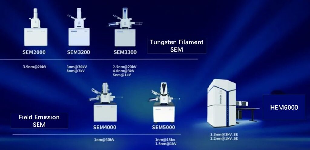
- Hansvue SEM2000: Basic analytical tungsten filament SEM. Resolution ~3.9 nm at 20 kV (SE), ~4.5 nm (BSE). Magnification up to ~300,000×. Supports optional accessories like BSE detectors, EDS.
- BSEM‑320A / BSEM‑320B: Resolution ~3 nm @30 kV in high vacuum (secondary electrons); somewhat lower at low voltages. Large sample chamber, three / five axis automated stage, multiple detectors. Used for metals, polymers, biological material, batteries, etc.
- Tungsten Filament SEM with 20 nm resolution: Developed in India by Bhabha Atomic Research Centre, over wide applications including material and alloy characterization, minerals, pharmaceuticals, etc.
Choosing a Tungsten SEM for Your Lab: What to Look For
If your institution is considering acquiring, upgrading, or using a tungsten filament SEM, here are factors to consider:
- Resolution vs Sample Type
What is the finest detail you need to resolve, and are your samples conductive / beam‑sensitive? If you often need sub‑5 nm resolution at low kV (to avoid charging or damage), the instrument must have exceptional optics, possibly advanced detectors, or support for low accelerating voltage. - Detectors & Analytical Tools
EDS for elemental analysis; BSE for compositional contrast; EBSD if you need crystallography etc.; additional detectors for photomicrography, cathodoluminescence if needed. - Vacuum System & Sample Environment
Can it handle low vacuum / variable pressure? Do you often need to image “wet” or non‑conductive biological or polymer samples? Environmental modes help. Also, chamber size and ease of loading large or awkward samples matter. - Stage & Accessibility
Multi‑axis stage, tilt, rotation; good working distance; accessibility for sample preparation; ability to observe cross sections, fracture surfaces, etc. - Cost & Maintenance
Consider not just purchase cost, but filament replacement, upkeep of vacuum system, detector maintenance, training of staff, and technical service. Tungsten filaments are less demanding than some alternatives, but there is still wear, drift, need for alignment, etc. - Software & Image Processing
Good software for image capture, stitching, contrast management, correction of astigmatism, drift correction. Also for quantitative work (e.g., EDS maps, line scans). - Utility in Your Research Environment
If your lab works in materials, semiconductors, biology, or environmental science, make sure that the instrument chosen meets the sample prep constraints, throughput demands, and detection/analytical requirements of your work.
Trends & Future Directions
- Improved Optics & Lens Designs that reduce aberrations and enable better image quality, especially at low accelerating voltages.
- Better Detectors and Signal Processing to improve signal‑to‑noise ratio, better contrast, easier acquisition of analytical data (EDS, EBSD), even in less ideal conditions.
- Variable / Environmental SEM Modes enabling imaging of less conductive, methodologically challenging samples without heavy coatings or harsh prep.
- Automation & Software Advances — automated focus, astigmatism correction, stage movement, image stitching, batch image acquisition to boost throughput.
- Competition with FEG/FESEM: pushes on lowering cost, increasing stability, bringing some of the advantages of FEG (brightness, small probe size) into tungsten SEMs or hybrid sources.
Conclusion:
Ultra‑high resolution tungsten filament SEMs provide a powerful, cost‑effective bridge between basic SEM imaging and the more expensive field emission alternatives. They are very well suited for many research labs—especially where routine imaging, material characterization, failure analysis, and quality control are needed. With good detector setups, excellent optics, and the right sample prep and environmental support, they can deliver impressive performance, often down to the few‑nanometer scale.
For labs evaluating such instruments, the key is to balance what resolution & analytical capability you truly need, what your sample types demand, and what maintenance & service capacity you have. When matched properly, a tungsten filament SEM can be a workhorse instrument—delivering vital insight into structure, composition, and surface morphology across disciplines.
Contact our experts for personalized equipment guidance, training, and SOP support.
Contact:
Email: sales@apex-instrument.com
Mobile/WhatsApp: +971526191767